top of page

The paper was published in Advanced Optical Materials.

Van der Waals (vdWs) heterostructures based on low dimensional semiconducting materials offer tremendous opportunities in investigating next generation electronic and optoelectronic devices. Careful design based on combinations of different crystal structures and their band alignment engineering in such architectures are crucial for realizing specialized functionality and preferable performance. Here, a polarized light sensitive photodetector with high efficiency and ultrafast response speed based on hybrid dimensional MoS2/Ta2Pd3Se8 vdWs heterostructure, which is owing to the unilateral depletion region as formed between the n–n junction, is reported. Our theoretical studies confirm this results. According to the theoretical analysis, a type-I band alignment will be formed between MoS2 and TPS when bringing them in physical contact, as displayed in Figure (a). At their interface, there possess a small energy offset of 0.28 eV between their conduction band and a large energy offset of 1.0 eV between their valence band. Then, we analyzed their energy band alignments under different bias conditions, as shown in Figure (b–d). At equilibrium state with Vds = 0 V, the electrons in MoS2 will transfer into TPS, forming a depletion region on the MoS2 side and accumulation region on the TPS side. In other words, a heterojunction with a unilateral depletion region is formed in MoS2 (Figure (b)). At a positive bias Vds > 0 V, both the heterojunction barrier and Schottky barrier become larger, and the electrons injected from the TPS side are hindered by the barriers, while a few holes are injected from the MoS2 side to flow, resulting in a small current amplitude (Figure (c)). When a negative bias Vds < 0 V is applied, both the heterojunction barrier and Schottky barrier decrease. Thus, the electrons are easily injected into MoS2 and pass through the heterojunction barrier and then flow to TPS, resulting in a large electron-dominated current as shown in Figure (d).


Band alignments of the MoS2/TPS heterostructure. a) Simulated band alignment between MoS2 and TPS. Energy band alignments and allowed charge flows of the MoS2/TPS vdWs diode at different bias, including b) Vds = 0 V, c) Vds > 0V, and d)Vds < 0 V. Note: the grey filled area indicates the unilateral depletion region in MoS2. The dashed lines denote estimated relative positions of the Fermi levels in MoS2 and TPS.


We believe that this work sheds light on the potential applications of hybrid dimensional vdWs heterostructures, which may provide new insight for exploring high performance photodetectors with advanced functions.

Updated: Jun 26, 2023

The application of nanoparticles to the surface modification of cotton fabrics is a promising approach to imparting a set of desirable characteristics to the material, allowing a significant increase in functionality, wearability and service life of textile products. Two approaches to surface modification of hexagonal boron nitride (h-BN) nanoparticles by treatment with maleic anhydride (MA) or diethylene triamine (DETA) were studied in the work published in ACS Applied Bio Materials.


Using DFT simulations, it was shown that the use of a coupling agent significantly increases the bonding strength of nanoparticles in the textile fabric. In addition, it was shown that the interaction of cellulose with boron nitride is much more effective than that with maleic anhydride when DETA is used. This hypothesis was confirmed in an experiment in which it was shown that the modernized boron nitride did not wash out after a day in water and after 40 washings.


Cotton fabric coated with the surface-modified h-BN nanoparticles has a high hydrophobicity. Compared with the original textile material, treatment with MA- and DETA-modified h-BN nanoparticles increases heat resistance by 10% (MA) and by 15% (DETA). Cotton fabrics coated with DETA- and MA-modified h-BN nanoparticles exhibit increased antibacterial activity against Escherichia coli U20 and Staphylococcus aureus strains and completely prevent E. coli biofilm formation. The results are important for the further development of fabrics for sports and medical clothing, as well as wound dressings.


The paper was published in Nanomaterials.

The prevailing surface contribution allows the modification of the multilayer graphene structure by surface functionalization which leads to the connection of the layers to form thinnest possible diamond film, diamane. Adsorption of reference atoms regulated by external conditions, by choosing appropriate temperatures and pressures, changes the structure of the film globally. However, this approach is not suitable when local manipulation of atomic geometry is required. It can be realized by using the biased enhanced nucleation approach allowing diamond nucleation by exposing direct electron irradiation of selected regions.

Use of electron irradiation for realizing of the chemically induced phase transition was demonstrated in our previous work where the induced formation of diamond nanocluster in the carbon network was shown. Hydrogen atoms displaced from the dodecyl groups by the “knock-on” effect penetrate the layered carbon and form a dense amorphous hydrogenated carbon (C:H) phase with the final precipitation of sp3 carbon clusters. It is attractive to extend this approach to the two-dimensional case, where an easily accessible surface allows local phase state tuning and enables the formation of a heterostructure consisting of regions with different conductivities. The latter can become the basis for nanoscale electronic devices.

The presented study is devoted to the investigation of the effect of chemically induced phase transition in bilayer graphene transferred onto a langasite substrate and irradiated with a focused electron beam through a layer of poly(methyl methacrylate). Transport measurements show that the resistance of the graphene bilayer after irradiation with an electron beam increases significantly, and the linear dependence of current on voltage in the bias voltage range from –1 to 1 V changes to a nonlinear one.

Our estimates show that the fraction of sp3 carbon in the irradiated region is about 10^12 cm–2 (see the figure below). When a certain local area of the sample is irradiated with a focused electron beam, hydrogen is released from the destroyed polymer on the one side, and oxygen from the langasite substrate on the other side. We suppose that active O and H atoms easily bind to the graphene surface which leads to the corrugation of the layer with displacing of the neighboring atom from the plane owing to sp3 hybridization. Such behavior of graphene is typical upon attachment of reference atoms to it. In the case of a single layer of graphene in this way, it is possible to obtain the “ultimate diamond slab” (graphane or fluorographene for the cases of H and F adsorption, respectively). The deposition of a reference atom to the carbon leads to the rehybridization of its bonding from sp2 to sp3, leading to a change in the chemistry of neighboring C atoms, that in turn tend to connect with other atoms. In the case of a multilayered film, such atoms are carbon atoms from the neighboring layer which leads to the bonding of the layers to each other and the final formation of a diamond film.


sp3 defect density distribution (cm-2) estimated from Raman D peak


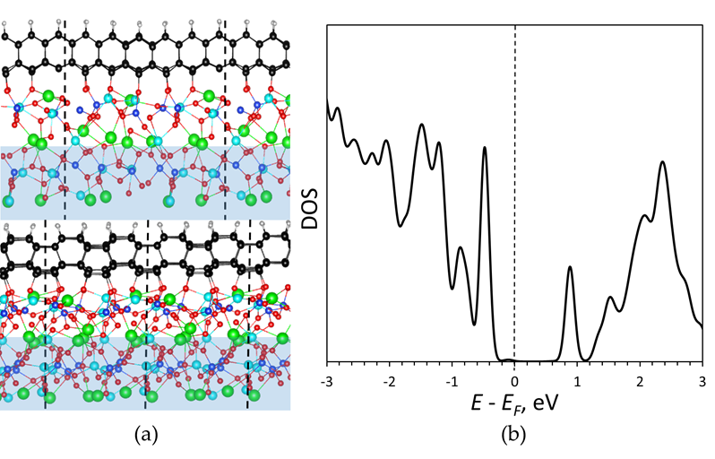
In the present case, graphene is exposed to oxygen atoms from one side and hydrogen atoms on the other side forming a Janus diamane structure. We designed the corresponding model of diamane film arranged on the LGS substrate functionalized by the hydrogen atoms from the outer side. During the relaxation surface oxygen atoms of langasite shifted and connected with the carbon atoms on the interface stabilizing diamane geometry. The final structure of hexagonal diamane film with the surface (see figure (a) given below) showed high stability which proves the experimental suggestion of bilayer graphene diamondization by treatment by H and O-atoms. Note, that the cubic diamane (111) structure was not stabilized by oxygen and was partially graphitized.

The observed high resistivity of the diamondized graphene regions is explained by the density of electronic states (see figure (b) given below) where formed diamane displays a band gap of ~0.7 eV. Thus, irradiation leads to the controllable formation of regions with the large barrier in the bilayered graphene. The smaller value of the band gap (in comparison with perfect diamane which band gap is more than 3 eV) can be explained by the presence of carbon atoms with unsaturated bonds at the interface not connected with oxygen.


a) Atomic model of a diamane film with surface which outer side is passivated by hydrogen atoms, and the other (at the interface) is connected with oxygen atoms of the langasite substrate. Carbon, hydrogen, oxygen, lanthanum, gallium, and silicon are marked by black, gray, red, green, cyan, and blue colors. Unit cell is depicted by dashed lines. The frozen region is marked by blue; b) Partial density of electronic states of the diamane (carbon and hydrogen atoms) from the diamane/langasite structure. The Fermi level is shifted to zero


It should be noted that the low sp3 carbon density observed in modified bigraphene indicates the formation of diamane nanocluster in irradiated area. It is probably caused by the non-optimal stacking of carbon atoms in two functionalized graphene layers, which is determined by the angle of rotation between the two layers. Other possible reasons are structural and technological defects that arise during the CVD growth of graphene and the process of transferring two layers of graphene onto a substrate. As calculations shown, not all bilayer graphene stacking can be transformed into diamane, so we can assume selectivity in the connection of twisted graphene containing areas with different packages. Therefore, fine control of structural and technological defects during the formation of the bigraphene/langasite structure and its irradiation with an electron beam are suggested to obtain high-quality diamane nanostructures. As a result, an experimentally observed barrier for the carriers transfer in the bigraphene/diamane/bigraphene nanostructure appears.

bottom of page