top of page

The paper was published in Nanoscale (2022).

Graphene oxide (GO) attracts significant attention due to its easily scalable and low-cost synthesis. GO was suggested as an attractive material for numerous applications in sensing, energy storage, 2D electronics and optoelectronics, photocatalysis, and memristors. This great tailorability of GO properties is apparently due to a rich variety of possible chemical compositions and structures. To further extend GO practical applications, it is highly important for the whole GO community to sort out the connections between a chemical composition, an atomic structure and electronic properties of GO.

In this paper we presented the results of our complex computational study of graphene oxide as a material with widely tunable structure and electronic properties. Using density-functional calculations, we considered various phases of fully oxidized GO and determined the most favorable structures among them. For the three selected stoichiometries, armchair and zigzag graphene nanoroads were paved in GO, and their thermodynamical, electronic, and magnetic properties were thoroughly studied for a broad range of nanoroad widths.

We showed that graphene nanoroads form highly stable, low-energy interfaces with GO and demonstrate the non-trivial dependence of electronic properties on a nanoroad width. Armchair nanoroads (Figure (a)) are characterized by the oscillating decrease of the band gap when widening a nanoroad (Figure (b)), and the same trend was observed for the charge carriers’ effective masses with their lowest values being in the range 0.05 – 0.2me for wide enough nanoroads (Figure (b), inset) that sounds promising for applications of patterned GO as a 2D semiconductor. Our results provide a possible explanation for the wide range of GO band gaps observed experimentally.

The electronic properties of zigzag nanoroads (Figure (c)) were found to be intimately connected to their magnetic state. Non-magnetic and ferromagnetic states are metastable and lead to a metallic conductivity, whereas antiferromagnetic arrangement was found to be a semiconducting ground state for zigzag nanoroads (Figure (d)). We have also demonstrated that AFM zigzag nanoroads can change their conductivity from a semiconducting to a half-metallic type when subjected to the external electric field.
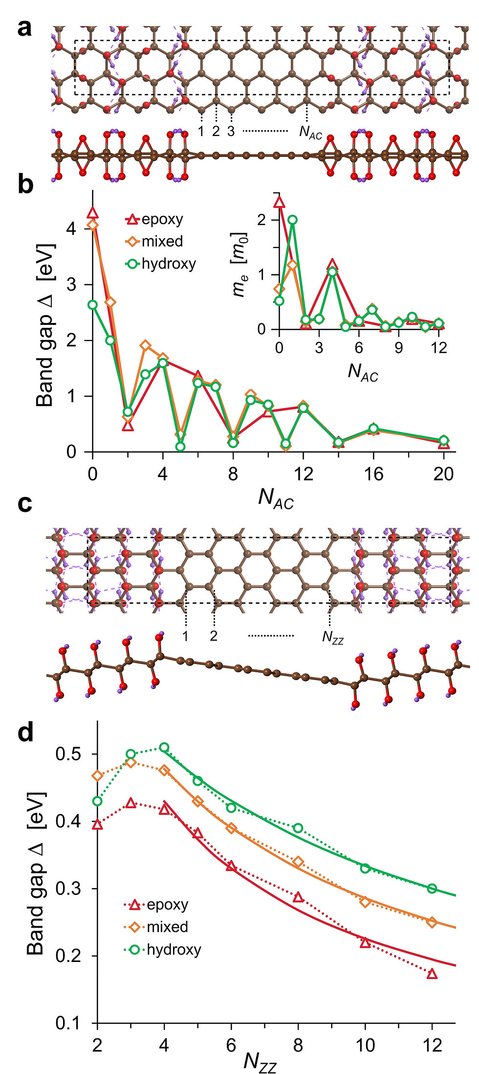
a) The atomic structure of 8-mixed-AGONR’ (top and side views are given). The dashed box shows the orthorhombic unit cell used in calculations. The numbers (1, 2, 3, …, NAC) indicate the number of dimer lines constituting the nanoroad width. b) The dependence of AGONR’ band gap Δ on the nanoroad width NAC for the three considered GO compositions: epoxy-GO (red), mixed GO (orange), and hydroxy-GO (green). The inset shows effective masses and electrons as the function of AGONR’ index. c) The atomic structures of 6-hydroxy-ZGONR’ (top and side views). The dashed boxes denote the orthorhombic unit cells used in calculations. The numbers (1, 2, …, NZZ) mark zigzag carbon chains making up a graphene nanoroad. d) The dependence of antiferromagnetic ZGONR’ band gap Δon the nanoroad width NZZ. The fitting (starting from NZZ = 4) with the hyperbolic law is shown with solid lines of corresponding colors

All mentioned effects are manifested very similarly for all three GO stoichiometries, which allows us to conclude that the electronic properties of GONR’ are mainly determined by graphene regions and weakly depend on the exact chemical composition of the GO matrix. In principle, this should relieve experimentalists from the need to thoroughly control the composition of the synthesized patterned GO without losing its remarkable electronic properties. Together with its cheapness and wide availability, this means that GO could finally become a material where graphene nanoroads with their exciting electronic properties can be observed and measured experimentally.

We believe that using state-of-the-art experimental techniques, such as STM, electron beam irradiation and nanolithography, it should be possible to create graphene nanoroads. Although currently there are no direct evidences for graphene oxide, we believe that these methods successfully applied to hydrogenated and fluorinated graphene can be generalized onto the case of oxygen groups as well. We assume that our theoretical predictions may serve as a good motivation for experimentalists to go in this direction, since the possibility to transform GO into a semiconducting structure demonstrated in our work has a great potential for practical applications. We hope that our results would be useful for people working in the GO community and beyond.

Updated: Aug 22, 2022

The paper was published in Diamond and Related Materials.

The nanostructuring of 2D materials has attracted increasing attention recently due to its wide variety of applications, including field-effect transistors, photonic and photovoltaic devices, biosensors, analyzers of biomolecule properties, storage devices, advanced materials, and microelectromechanical systems. The creation of nanoporous layers is an important tool for the modification of 2D material properties.

In the present study, we have revealed the possibility to modify the parameters of few-layer graphene and, first of all, the size of the pores as a function of ion irradiation energy and pristine graphene structural features, and morphology. The maximum pore density is approximately equal to the ion dose found in blisters. The pore size depends on the size of the domains in graphene and ion energy. The formation of more complex structural defects in few-layer graphene is also observed after irradiation. Thus, the use of CVD graphene provides opportunities for controlling the structure and properties of the material modified by high-energy ions.


Typical graphene structure after the irradiation by Xe ion with energy a) 167 MeV and b) 100 MeV. The size of the formed pore is ~ 5×5 nm2. c,d) Behavior of the amorphized carbon ribbon, periodic only in the direction perpendicular to the figure plane (y-direction), under annealing conditions (see text for details).


We found that the decreasing of incident Xe energy from 167 to 100 MeV sufficiently change the behavior of the system. Irradiation with such energy leads to the structure amorphization with almost no evaporation of carbon from the structure. The amorphous carbon remaining in the structure can transform back into the sp2 system after cooling (healing effect), or it can change to other phase states, which are abundantly observed in the experiment.

Nevertheless, if we consider only a fragment of the edge of the multilayer graphene structure (Figure b) next to the ion track and perform long-term molecular dynamics, we can get some idea of what happens in the irradiated material already during cooling. Figure 9c shows an amorphized carbon ribbon, periodic only in the direction perpendicular to the figure plane (y-direction), with a cell parameter equal to 4.84 Å. The carbon atoms on the left edge of the ribbon are grouped and connected to the "cold" multilayer graphene thermostat at room temperature. The atoms on the right side are respectively grouped and connected to the thermostat of the material in the area of the track just after the irradiation at a temperature of 4000 K. Molecular dynamics are then performed for a few nanoseconds, during which time the temperature in the track decreases and the carbon in the middle of the ribbon is annealed and transformed into more favorable phase configurations. After a series of calculations, where the initial amorphous structure and cooling time were varied, it was observed that most of the transition of the resulting structure to sp2 hybridization of the carbon on the surface of the ribbon (Figure d). This effect can explain the stability of the outer graphene layer in the FLG irradiation experiments. The Xe ion must transfer noticeably less energy to the outer layer than to the inner layers because of the cascade effect, which is also applicable to electron stopping. The inner layers are exposed not only to the ion but also to the electrons knocked out of the previous layers, which adds up to the value of the average ion loss for ionization. The outer layer is only affected by the ion, so the energy transferred may not be enough to evaporate the carbon from the outer layer, and the amorphized structure may heal into graphene over time, as occurs in the numerical simulation. This could explain the observation of formations in few-layer graphene with the undistorted outer layer in the places of ion incidence.


The paper was published in Nano Letters (2022)

This work was done in collaboration with a team from Queensland University of Technology supervised by Prof. D.V. Golberg.

Two-dimensional (2D) inorganic nanomaterials have been extensively studied. These include graphene, boron nitride, silicone and beyond, transition metal dichalcogenides (TMD), transition metal oxides, perovskites, and MXenes. 2D nanomaterials have shown diverse electromechanical and optoelectronic properties. They are promising for strain-engineered applications (e.g., strain sensors, flexible energy storage, flexible diodes, transistors, detectors, and diagnostic devices).

A photodetector fabricated with the partial vertical heterojunction between MoSe2 and Si has also been introduced. However, the effects of “edging” deformations (i.e., those with a loading axis parallel to the 2D basal atomic planes) on optical and/or optomechanical performances of layered nanomaterials have not been studied.

These drawbacks can be addressed via in situ high-resolution TEM (HRTEM) experiments using an optical TEM holder. In this paper, we define the deformation perpendicular to the

2D material layers’ basal atomic planes as a bending deformation, whereas the deformation parallel to such planes is called as an “edging” deformation.

Two MoSe2 atomic models were considered to understand difference between bending and edging deformations via DFT calculations. For convenience, an elastically bent MoSe2 monolayer was represented as a single-wall nanotube with a uniform curvature, whereas for edging deformation we simulated MoSe2 as an undulated monolayer defined by a wavelength and wave amplitude.

Series of consecutive TEM images illustrating a (a−c) bending and (e-f) edging deformation experiment on a MoSe2 nanosheets’ stack. (f) Characteristic TEM image of the nanosheet stack after severe edging deformation

Our findings correlate with experiments. For the case of bending deformation on the basis of TEM (Figure (a−c)), we see a general preservation of the initial MoSe2 structure under elastic bending. Moreover, since the photocurrent spectroscopy shows no difference between the deformed and undeformed MoSe2, we conclude that the valence band is mainly unchanged.

The DFT results also correlate with the experimental data for edging deformation, such as damage of MoSe2 surface (figure (f)) and highly unstable currents. Local high curvature and drastic structural alterations in flex points result in CBM and VBM changes. Band gap reduction and transition from a direct to indirect mode become apparent. Fracture of monolayered MoSe2 under high strains is attributed to its flexural rigidity, an order of magnitude greater than that of graphene. Nevertheless, even this damage is reversible for the monolayer case, while in thicker TMDs films, cracks and kinking appear and further accumulate under strain cycles. The latter can explain gradually rising current each cycle following the calculated monotonous band gap decrease

bottom of page